Research Highlights
Semiconductors Enter the “Multi-tasking” Era: New Device Cuts Required Components by 75% and Quadruples Processing Speed
- Electrical Engineering Semiconductor Engineering
- Date2026.06.04
- Views1853
[POSTECH develops a low-temperature heterojunction-based transistor that implements complex circuits with a single device]
Less than two decades after smartphones fit into the palm of our hands, artificial intelligence is now running on devices worn on our wrists. The challenge is that while devices continue to shrink, the amount of data they must process and the number of functions they must perform are growing exponentially. A research team at POSTECH has found a promising way to address this contradiction.
A team led by Professor Byoung Hun Lee of the Department of Electrical Engineering and the Department of Semiconductor Engineering at POSTECH, together with Dr. Jae Hyeon Jun of the Department of Electrical Engineering, has developed a transistor technology that enables a single semiconductor device to perform multiple circuit functions simultaneously. The new approach significantly simplifies circuit design and increases data processing speed by fourfold compared with conventional methods. The findings were published in Advanced Functional Materials, an international journal in the fields of materials science and electronic devices.
One of the key challenges in the semiconductor industry is integrating more functions into smaller chips. As the number of functions increases, so do the number of circuits and transistors required. However, when adding new functions to previously fabricated semiconductor chips, back-end-of-line(BEOL1)), processing must be conducted at temperatures below 400°C to protect the existing chip structure.
The research team focused on zinc oxide(ZnO) and tellurium(Te). Both materials can be fabricated as thin, uniform films at temperatures below 200°C, making them promising candidates for next-generation semiconductor materials. By combining the two, the team created a ZnO–Te heterojunction2) transistor.
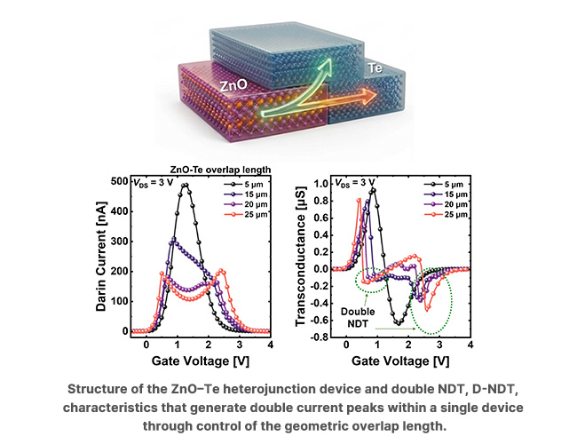
The device controls current flow in a highly distinctive way. Unlike conventional semiconductors, in which current generally increases as voltage rises, this device exhibits negative differential transconductance(NDT3)), in which current decreases over a certain voltage range. The team successfully realized double negative differential transconductance(D-NDT4)), in which this phenomenon occurs twice in succession within a single device. In simple terms, the technology allows a single device to handle tasks that would normally be divided among multiple devices, thereby reducing circuit complexity.
The key lies in precisely controlling the overlap length between the two materials. When the overlap region is short, the current changes only once. However, as the overlap region becomes longer, both lateral and vertical currents form simultaneously within the device, generating double current peaks. Just as a current flowing in a straight line becomes capable of more complex routing when it meets a three-dimensional intersection, the device becomes capable of more complex signal processing.
Using this device, the team implemented a frequency quadrupler5) that converts one input signal into four output signals. This function would typically require multiple transistors, but the new technology achieves it with a single device, reducing the number of required transistors by 75%. In actual circuit experiments, the researchers also confirmed that data processing speed increased fourfold within a single input signal cycle.
“This study demonstrates the possibility of implementing complex circuit functions at the level of a single device,” said Professor Byoung Hun Lee. “We expect this technology to be widely applicable to the development of ultra-compact AI devices and three-dimensional integrated, highly-density semiconductor systems.”
This research was supported by the Core Technology Development Program for the National Semiconductor Research Laboratory and the Nano-materials Technology Development Program, funded by the Ministry of Science and ICT and the National Research Foundation of Korea.
▶️ DOI: https://doi.org/10.1002/adfm.74948
1. BEOL, Back-End-Of-Line: BEOL refers to the back-end process in semiconductor manufacturing, in which metal interconnects are formed. The device developed in this study is fabricated at temperatures below 200°C, making it compatible with BEOL processes and three-dimensional integration technologies.
2. Heterojunction: A heterojunction is a device formed by combining two semiconductors with different properties. In this study, n-type ZnO and p-type Te are combined to create unique nonlinear electrical responses by utilizing their different charge transport characteristics.
3. NDT, Negative Differential Transconductance: NDT is a phenomenon in which current decreases after a certain point as gate voltage increases. Because it exhibits nonlinear behavior unlike ordinary transistors, NDT is advantageous for specialized circuit applications such as frequency multiplication and multi-valued logic.
4. D-NDT, Double Negative Differential Transconductance: D-NDT refers to the appearance of double NDT peaks in the transfer characteristics of a single device. As an input signal sequentially passes through these double peaks, the device can generate multiple output responses within a single cycle, enabling higher-order frequency conversion.
5. Frequency Quadrupler: A frequency quadrupler is a circuit or device that converts an input frequency into an output frequency four times higher. While this function generally requires multiple devices and complex circuit configurations, the present study demonstrates it using a single-stage device.
Researcher
-

Lee Byoung Hun Professor
Dept. of Electrical Eng.
View Profile -

JaeHyeon Jun
Dr.